IDAX Serves

Interconnect (at chip level, between chips and substrate)
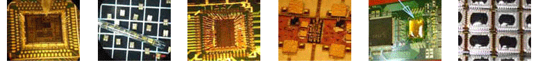
     • Wire-Bonding
        Wedge Bond & Ball Bond;
        Alum wire 0.7~2.0 mil Dia, Gold wire 0.7~1.0 mil Dia.;
        Pad size down to 2.5 x 2.0 mil;
        Gap between pads >= 0.5 mil
     • Flip Chip
        Chip size =< 5 mm square
     • Attach SMDs
        Soldering, down to size 0402, 0201

Design
     • Packaging design, Semi-conductor & Microelectronic Device
     • Board layout
     • Design for Manufacturing

Assembly
     • Device Packaging
       Open-Cavity Package DIP, SO, TO, LCC, QFP, QFN, PGA
     • Microelectronic Packaging
       COB, COF, Microwave Device, Hybrid

Related Services (X)
     • Engineering Experiments
     • Open/Short Test
     • Wire Pull Test, NPT or DPT
     • Manufacturing methods R&D
     • Small process machine design & development
     • Clean-Room design

Customer Testimonial

C. Hendrick, CEO, SmartMetric

... thank-you note ... contributing vital manufacturing
suggestions to our products ... to success
  
  
Better Packaging Process
  • Design the substrate & up it to
    "Design for Manufacturing"

  • Incoming Inspection
  • Design & fab Fixture on-site
  • Attach passive components
  • Die-Attach; conductive or non-conductive epoxy
  • Wire-Bond, e.g. Alum wire, Gold wire;

  • Electric Open/Short Test, per Ur procedures
  • Wire Pull Test, NPT or DPT, w/Statistic Data
  • Encapsulation, optical clear or black opaque
  • Attach SMDs, if required
  • Outgoing Electric Test, per customer procedures
We Contribute the Best Visions & Values!
 
 
COB@idaxlabs.com    /   Recommend Us To A Friend