| To: AAA ¨C Engineer, Broadcom |
| From: BBB - IDAX Microelectronics |
| Report Date: |
| |
|
| Subject: Assembly Report ¨C Microwave Device |
| |
| |
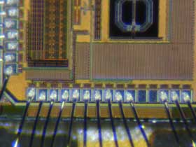
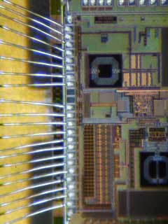
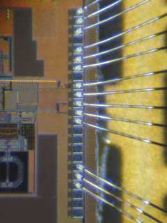
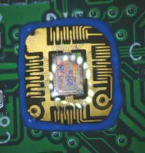
| Job Scope |
Chip-On-Board Packaging, 5 Boards |
62 wires/board x 5 boards |
| Wedge bond, Alum 0.7 mil |
| 2 Critical Wires of equal length |
|
|
|
| |
|
| |
|
| |
| |
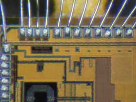
| Incoming Board surface |
Observation:
Many short fibers around SMDs corners |
Reason:
Probably caused by the soldering operator using paper to wipe off the residual of solder flux |
Risk:
Electric short |
IDAX Action:
Use tape adhesive to Get those fibers off the board |
Suggestion:
Remove fibers after wiping the flux Thoroughly with tape adhesive |
|
|
|
|
| |
|
|
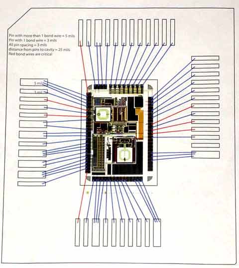
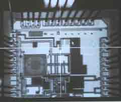
Bonding Diagram |
|
| |
| |
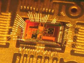
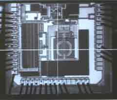
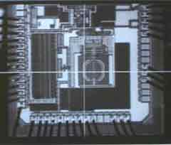
2. First Unit: Not Encapsulated Yet |
|
| |
| |
| Preparation |
Tagged each board with a number from #1~#5 |
| Attach die while constrain epoxy within the die size |
Setup on
W/B work-stage |
Ground during Wire-Bond Operation |
|
|
| |
|
| |
|
| |
|
|
|